Updated:
VHDL IP: AD7823
Chip Description

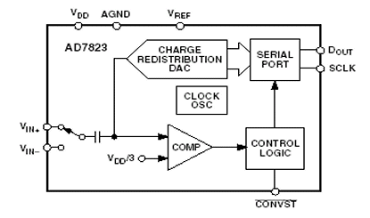
The AD7823 is an 1-channel 8-bit DAC with a synchronous serial interface. It seems that the most appropriated solution to interface this device is to use a FSM and a shift register. The maximum ADC sample rate is 200 kSPS, enough for audio applications.
Ports and Usage
The macro has the following ports:
| Port | DIR | Type | Description |
|---|---|---|---|
| reset | Input | signal | Asynchronous reset |
| clk | Input | signal | Clock signal (> 30MHz) |
| clk10MHz | Input | signal | Slow clk for internal macro use (measure time) |
| start | Input | signal | Start ADC conversion |
| eoc | Output | signal | End Of Conversion, it's a "ready" signal that notifies that the conversion has ended and it is possible to order a new conversion |
| do | Output | 8-bit bus | The 8-bit sample read from AD7823 |
| di | Input | signal | Serial data input from AD7823 |
| sclk | Output | signal | Control signal for AD7823 (clock signal) |
| convst | Output | signal | Control signal for AD7823 (initiates the ad7823) |
The circuit waits the start signal to initiate the conversion and puts the acquired 8-bit sample
after 5 us (250 system clock cycles @50MHz).
After power up the circuits, wait at least 6 us. Then assert start and wait for eoc to
go 1 (only for one clk cycle, use it as a interrupt signal if you want), the acquired 8-bit sample
will be present at do port. Repeat as many times as you want.
Block Diagram And Control State Machine
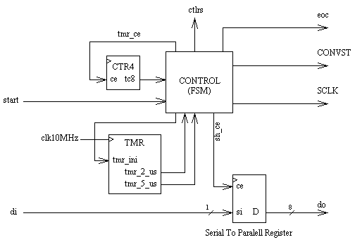
The figure depicted below shows the RTL block diagram of the circuit. All sequential blocks share the same asynchronous reset and clock signals. The control finite state machine (FSM) has 11 states, there are 7 control signals for datapath.
Datapath

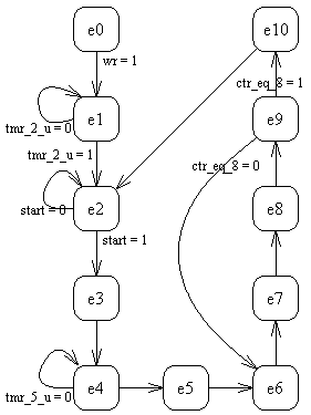
Control

| State | ctlrs | ctr_ce | sh_ce | tmr_ini | eoc | sclk | convst |
|---|---|---|---|---|---|---|---|
| e00 | 1 | 0 | 0 | 0 | 0 | 0 | 1 |
| e01 | 0 | 0 | 0 | 0 | 0 | 0 | 0 |
| e02 | 1 | 0 | 0 | 0 | 0 | 0 | 0 |
| e03 | 0 | 0 | 0 | 0 | 0 | 0 | 1 |
| e04 | 0 | 0 | 0 | 0 | 0 | 0 | 0 |
| e05 | 1 | 0 | 0 | 0 | 0 | 0 | 1 |
| e06 | 0 | 0 | 0 | 0 | 0 | 1 | 1 |
| e07 | 0 | 1 | 1 | 0 | 0 | 1 | 1 |
| e08 | 1 | 0 | 0 | 0 | 1 | 0 | 1 |
| e09 | 0 | 0 | 0 | 0 | 0 | 0 | 1 |
| e10 | 1 | 0 | 0 | 0 | 1 | 0 | 1 |
The FSM has the following graph, state after reset is e0, the control signals in each state are shown in the table. The signals printed in green are registered because random effects on this signals could cause a malfunctioning of entire system (AD7823 expects inputs free of spurious transitions)
Synthesis Report
    Device xc3s400-4ft256

    slices=22
    ff=28
    lut=41
    ob=16
    gclk=2
    maxfreq=200.942MHz
Download
- ad7823.vhd
- ad7823_test.vhd. A test bench for simulation
- utils.vhd. A package with some useful routines