VHDL IP: VGA80x40
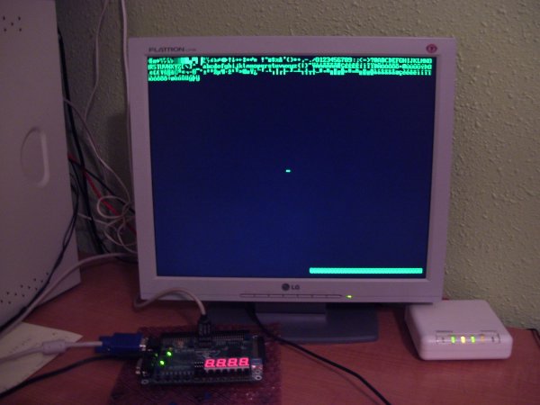
This VHDL macro is a Text Mode Monochrome Video Display Adapter intended to be used as a PicoBlaze (or other CPU) peripheral. It's not much better than the original IBM MDA card appeared in 1981 :-)
- resolution of 80x40 characters, dot resolution is 640x480 pixels at 60Hz so the core needs a clock signal of 25 MHz. I prefer 80x40 instead the classical 80x25, in my opinion, the latter is an annoyance.
- monochrome, it hasn't "attribute" memory to store the colour of each character. The unique output color is selectable among 8 different colours
- 8-bit ASCII codes (iso-latin-0 or other that you prefer)
- the video text buffer is an external memory of 80 x 40 = 3200 bytes. The character at (column, row) = (0, 0) is at the RAM address 0, the character at (79, 39) is at 3199.
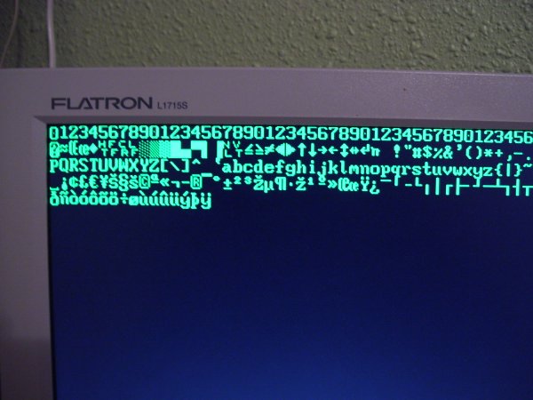
- the ROM that store fixed-width bitmap font is also external, the bitmap can be changed modifying the COE file. The COE file provided is iso-8859-15 (also called iso-latin-0), is very similar to the iso-8859-1 but with the euro (€) symbol added.
- hardware cursor, with two different shapes; with enable/disable control.
- simple IO interface. Three registers
- CRX. Position (column) for HW cursor
- CRY. Position (row) for HW cursor
- CTL. Control register for de/activate the HW cursor, change its shape, de/activate VGA signal, output colour, etc.
- uses 100 slices in a Xilinx Spartan-3.
- the design is vendor-agnostic. You can use it in Xilinx/PicoBlaze, Altera/NIOSII, etc

|

|
Ports description
| Port | Dir | Type | Description |
|---|---|---|---|
| reset | Input | signal | Asynchronous reset |
| clk25MHz | Input | signal | Clock signal. 25MHz is the pixel clock for the resolution used |
| R | Output | signal | Red color component |
| G | Output | signal | Green color component |
| B | Output | signal | Blue color component |
| hsync | Output | signal | Horizontal sync signal for the VGA monitor |
| vsync | Output | signal | Vertical sync signal for the VGA monitor |
| TEXT_A | Output | 12-bit bus | Address bus for RAM Video Text Buffer |
| TEXT_D | Input | 08-bit bus | Data incoming from RAM Video Text Buffer |
| FONT_A | Output | 12-bit bus | Address bus for ROM font buffer |
| FONT_D | Input | 08-bit bus | Data incoming from ROM font buffer |
| CRX | Input | 08-bit bus | X (column) position of HW cursor. |
| CRY | Input | 08-bit bus | Y (row) position of HW cursor. |
| CTL | Input | 08-bit bus | Control of the peripheral. Bit 7 (MSB) is VGA enable signal. Bit 6 is HW cursor enable bit. Bit 5 is Blink HW cursor enable bit. Bit 4 is HW cursor mode (0 = big; 1 = small). Bits(2:0) is the output color. |
This macro, therefore, needs two external memories to store text and font data not included in the
source files package. This memories must be created by you using, for example, Xilinx CORE Generator or an
equivalent tool from other vendor
You can also define them in pure VHDL and let synthetizer to recognize them as BRAM memories but this way
is not recommended
. The lat0-12.coe file contains the data for the font ROM memory. View a complete example of how to
use this macro in The Game Of Life for PicoBlaze.
Interface with a VGA monitor
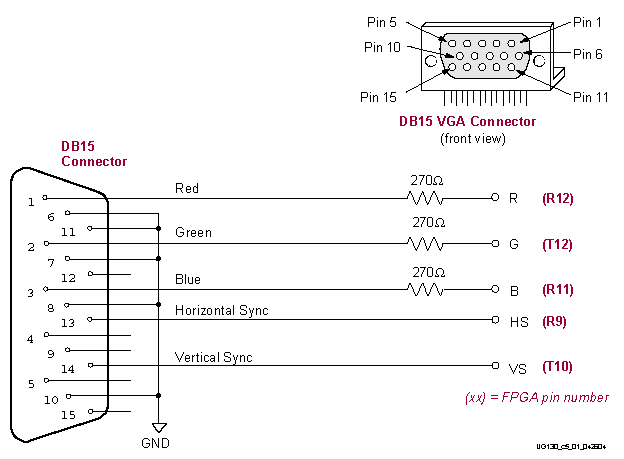
The electrical interface between FPGA and the VGA monitor is very simple, only 3 resistors of 270 $\Omega$ are needed. The following figure is extracted from S3Board manual from Xilinx (S3Board is the development FPGA board that I use)

The input impedance of every signal (R, G B, HS and VS) line is 75 $\Omega$ (like TV). The analog video signal is obtained simply thought a 270 $\Omega$ resistor (1-bit DAC) for R, G and B signals. With a digital output of 3.3V (I assume a LVCMOS33 IO STANDARD for your FPGA pin) the analog voltage outputs are:
- with logic "0" at FPGA pin the analog voltage is 0 V, that represents black for that colour
- with logic "1" at FPGA pin the analog voltage is $3.3V * 75\Omega / (75\Omega + 270\Omega) = 0.71V$ that represents maximum bright for that primarily colour (R, G or B)
The FPGA (or CPLD) normally can drive the VGA signals directly, there's no need of voltage buffer nor other
special
hardware. The maximum bright in a R, G or B signal is represented by 0.7 V. If you use other IO standard like
LVCMOS
2.5V, obviously you need to use smaller resistors. With this 3 resistors only 8 colours can be obtained, you can
select
the output colour among the 8 possible ones with the CTL(2:0) register.
For VGA signal format information, see [[VGA Video Signal Format and Timing Specifications]].
Cheat: One Unique Output Colour
If you can't afford to use 3 FPGA pins for R, G, B signals then connect only one output pin (R, G or B) to the 3 resistors to obtain a nice white output colour, it will be the only possible output color. This saves 2 FPGA pins. By other hand, to achieve a less brilliant colour, put bigger resistors so that the analog video signal level is below $0.7 V$.Interface with PicoBlaze
The interconnection with PicoBlaze is as usual, like any other peripheral:
- Define output (for OUTPUT instruction) registers for ''CTL'', ''CRX'' and ''CRY'', decode port_id and write_strobe signal to assert register's ce control signal.
- Add TEXT and FONT RAM memories. The RAM addresses generated by this macro are ready at least 6 clock cycles (f=25MHz) prior the data is transferred, so the timing shouldn't be a problem, simply assert memory's enable pin forever
Synthesis report
| device | xc3s400-4ft256 |
| slice | 100 |
| ff | 76 |
| lut | 190 |
| iob | 67 |
| gclk | 2 |
| mfreq | 141.965 MHz |
Download
![]() The file if_vga80x40.zip contains all
the design files plus scripts and
font.
The file if_vga80x40.zip contains all
the design files plus scripts and
font.
2008-09-20 Update: Alessandro was kind enough to send me a patch to fix a little misalignment in the first screen's column. To apply the fix (I have no tested it yet) replace the original vga80x40.vhd file by vga80x40_col1fixed.vhd included in the zip file. Thank you Alessandro.
Obtain A Fixed-Width Console Font
VGA80x40 part stores in a ROM (for example a read-only Xilinx BRAM) the bitmap of each character associated with each ISO-LATIN-1 code (8-bits). You can choose other coding scheme if you want.
Where can we obtain a console font?
Using a font editor you can draw your own characters but it's easy to take an already made one. Linux [ftp://ftp.win.tue.nl/pub/linux-local/utils/kbd/ kbd package] comes with many console fonts (fixed-width bitmap fonts) in the folder /data. The PSF (Poscript Font) format is easy to understand and it's documented in de /doc directory of the package.
The provided ruby script psf2coe.rb translates PSF1 format file into Xilinx COE file to store the
console fixed-width bitmap font in a BRAM inside the FPGA. If you want to render the *.psf file in a text file
or to do
the opposite operation (font editor) use [http://nafe.sourceforge.net/ NAFE].
| File | Description |
|---|---|
| lat0-12.psfu | Font file iso-8859-15 with 12 pixels heigh. |
| psf2coe.rb | Ruby script that translates PSFU to COE file format suitable to use with Xilinx ISE Webpack tools. |
| lat0-12.coe | COE file suitable for XilinX ISE. |
| lat0-12.txt | Font rendered in a text file using NAFE. |
Possible Enhances For The Macro
- Optional use of an "attribute" memory to display characters in different colours.
- TV out (monochrome composite signal or colour thought SCART port).
- Different resolutions (800x600px modes)
- etc
Although some of this features could be useful, I prefer to maintain this macro in a small size. This macro is not intended to compete with the ultimate 3d video card in the market but to be a small and useful peripheral for your FPGA projects.
References
- PSF file format
- VGA Timings
- VGA pinouts
- Conceptos básicos de arquitectura y sistemas operativos. Curso de ordenadores, Gregorio Fernández, 3º edición, ISBN 84-605-0522-7